A Metal-Oxide-Semiconductor Field-Effect Transistor, or MOSFET, is one of the most widely used types of transistors in modern electronics. It’s a three-terminal semiconductor device that can be used either as a switch or an amplifier. Understanding how MOSFETs work and their characteristics is vital for anyone working with electronics. In this blog, we will break down the MOSFET working principle and its key characteristics in easy-to-understand terms. It will serve as a helpful guide for beginners and serve as a refresher for experienced electronic engineers looking to polish their understanding of MOSFETs. So, let’s dive in!
1. Introduction to MOSFET
The MOSFET, or Metal-Oxide-Semiconductor Field-Effect Transistor, is a type of transistor commonly used in electronic devices for amplification and switching purposes. It was invented in the early 1960s and quickly gained popularity due to its high input impedance, low power consumption, and fast switching speed. The structure of a MOSFET consists of a metal gate separated from the semiconductor channel by a thin layer of insulating material. The three terminals of MOSFETs include the source, the drain, and the gate, which controls the flow of current through the channel. The semiconductor technology behind MOSFETs involves the use of silicon-based materials that allow for efficient and reliable performance. Overall, MOSFETs offer various advantages over traditional transistors and are widely used in modern electronics.
5. History of MOSFET Invention and Production
As discussed in the earlier sections, the history of MOSFET can be traced back to the pioneering research of Julius Edgar Lillenfeld and his patent in 1926 for a transistor. However, it was not until the 1940s that American scientists experimented with a metal-oxide-semiconductor field-effect transistor, which is now known as MOSFET. It was not widely used until the 1950s when patents and developments in Europe were presented. MOSFETs are generally manufactured using integrated technology on a single silicon chip, allowing for smaller and more efficient electronic components. Understanding the history of MOSFET invention and production provides valuable insights into the development of semiconductor technology and its impact on modern electronics.
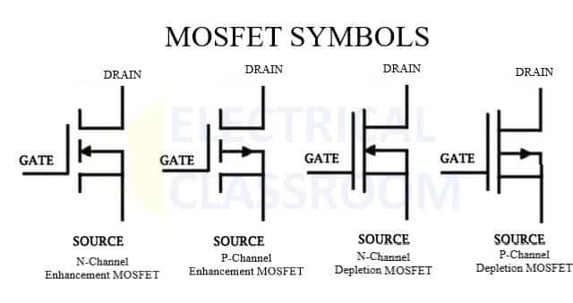
7. MOSFET Electronic Symbol and Characteristics
The MOSFET has a unique four-terminal device structure, consisting of a Drain (D), Source (S), gate (G) and a Body (B). Its electronic symbol is characterized by a semiconductive channel between the drain and source connections, known as the MOS capacitor. This channel can either be an n-type or p-type material, depending on the MOSFET’s design. When voltage is applied to the gate, it creates an electric field that alters the channel’s width, allowing or blocking the flow of charge carriers. This change in conductivity can be used for amplifying or switching electronic signals. Thanks to the metal-insulator-semiconductor structure, it possesses high input impedance, low output impedance, and is highly efficient. By understanding the MOSFET’s electronic symbol and characteristics, it can be utilized in various industries beyond electronics, including power systems and renewable energy.
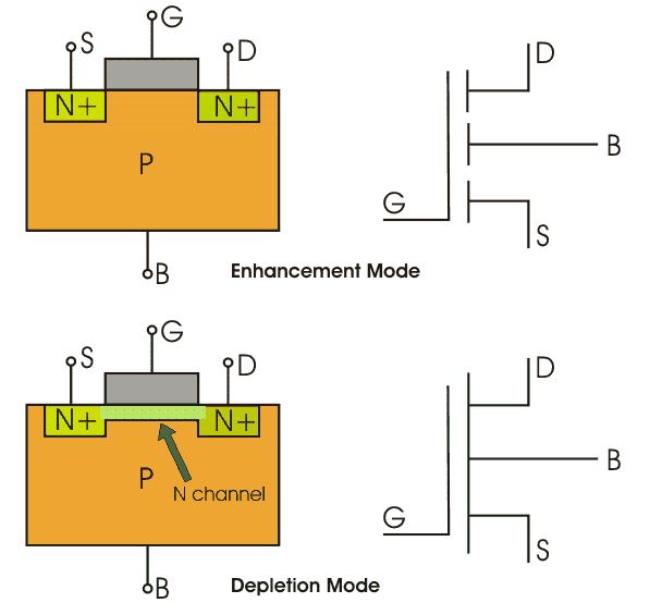
2. MOSFET Structure and Terminals
The structure of a MOSFET includes three terminals, namely the source, gate, and drain. The source and drain terminals are made of highly doped regions and are connected to the conducting channels created by the gate voltage. The gate terminal, on the other hand, is made of a thin insulating layer over the channel, separated by a layer of oxide. The gate voltage determines the conductivity of the device by controlling the formation of an inversion layer in the channel region, thereby controlling the current flow between the source and drain terminals. The MOSFET structure is highly versatile and can be modified to suit specific requirements of voltage and current ratings. The MOSFET structure and terminals are crucial to understanding the working principles and characteristics of the device, including its electronic symbol and driving methods.

8. Working Modes of MOSFETs
The working modes of MOSFETs are an important aspect to understand for any electronic engineer. In general, MOSFETs work as switches that control the voltage and current flow between the source and drain terminals. They can operate in three different modes: cutoff, triode, and saturation. The cutoff mode is when the device is completely turned off, and no current flows between the source and drain terminals. The triode mode is when the MOSFET operates like a linear resistor, and the current flow is proportional to the gate-source voltage. The saturation mode is when the MOSFET acts as a short circuit, and the current flow is limited by the external circuitry. Understanding the different working modes of MOSFETs is crucial to designing efficient electronic circuits. This section is closely related to the previous ones on the structure and operation principle of MOSFETs, as it builds upon that knowledge to explain how the device can be used in different applications.
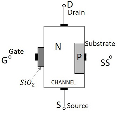
3. MOSFET Operation Principle
The operation principle of a MOSFET is a crucial part of understanding the device. As discussed earlier, a MOSFET works as a switch, controlling the voltage and current flow between the terminals. When voltage is applied to the gate, it generates an electrical field, changing the width of the channel region. As a result, a current flows between the source and drain terminals, and the device turns on. The MOSFET operation is dependent on the construction of the device, which is similar to a FET. The substrate has an oxide layer on which the gate terminal connects, and the metallic gate terminal is insulated from the semiconductor layer by a dielectric layer. Understanding the operation principle and the construction of a MOSFET is crucial in understanding its characteristics and electronic symbol representation.
6. Semiconductor Technology behind MOSFET
Semiconductor technology has a significant influence on the development and production of MOSFETs. As the demand for more advanced and efficient electronic devices increases, MOSFETs are inevitably becoming smaller and more complex. Miniaturization of MOSFETs is made possible by developments in the semiconductor industry, which provides the foundation for these devices’ structure and operation. The widespread use of silicon in semiconductor fabrication paved the way for MOSFETs, and it remains a popular choice for semiconductor components production. The technology used in processing semiconductor materials, such as etching, doping, and packaging, is key to achieving the desired characteristics of MOSFETs. Furthermore, innovative technologies like SiC FETs are emerging in the market, presenting new possibilities for more efficient and compact electronic devices. The evolution of semiconductor technology behind MOSFETs has enabled the production of highly-functional integrated circuits and improved performance of electronic devices.

9. IGBTs and MOSFETs: Comparison of Driving Methods
The previous sections of this blog discussed MOSFET structure, operation principle, and electronic symbol and characteristics. Now, it is time to compare IGBTs and MOSFETs in terms of their driving methods. IGBTs are commonly used in high power applications such as motor drives and power supplies. They have a higher current density and lower on-state resistance compared to MOSFETs. However, IGBTs have a slower switching time, resulting in more switching losses. On the other hand, MOSFETs have faster switching times and lower conducting losses, making them more efficient for low voltage applications. It is important to consider the specific application requirements when choosing between IGBTs and MOSFETs. Understanding the differences between the driving methods will enable designers to make informed decisions in selecting the right components for their projects.
10. Final Thoughts
In conclusion, understanding the working principle and characteristics of MOSFETs is important for anyone involved in electrical engineering or related fields. MOSFETs are particularly useful in power electronics due to their low power consumption, high switching speed, and ability to handle high voltages. The invention and production of the MOSFET in 1959 and 1960 respectively marked a significant milestone in the development of electronic devices. The modern MOSFET has complex characteristics, which are more advanced than the simple algebraic model that is often used to describe their operation. It is important to note that driving MOSFETs and IGBTs require different methods, so it is crucial to choose the right device for a particular application. Ultimately, the MOSFET is an essential component of electronic circuits, and understanding its operation can lead to the development of efficient and innovative electronic designs.